The semiconductor manufacturing process involves a series of essential steps, each requiring specialized machine tools. These steps are categorized into the front-end and back-end processes.
Parker engineers work in close partnership with machine tool manufacturers to create cutting-edge semiconductor manufacturing equipment. The tool hook-up process, which entails installing and integrating this equipment with the necessary utilities and systems in the fabrication facility, is vital for the proper functioning of these tools. Precision in this process is critical to ensure the equipment operates correctly and safely.
FRONT-END PROCESS
The front-end process involves the initial stages of semiconductor manufacturing, where raw silicon wafers are processed to create integrated circuits.
- Deposition: Thin films of materials are deposited onto a wafer using techniques such as Chemical Vapor Deposition (CVD) or Physical Vapor Deposition (PVD). These films form the layers that will be patterned.
- Photoresist Coating: A light-sensitive material called photoresist is applied to the wafer. This coating will be patterned during lithography.
- Lithography: The wafer is exposed to UV light through a photomask, transferring the desired pattern onto the photoresist. The exposed (or unexposed) areas become soluble in a developer solution.
- Baking and Developing: Post-exposure baking enhances the photoresist's properties, followed by developing, which removes the soluble parts of the photoresist, revealing the pattern.
- Etching: The exposed areas of the underlying material are etched away using either wet or dry etching techniques, transferring the pattern from the photoresist to the wafer.
- Ion Implantation: Ions are implanted into the wafer to modify its electrical properties, creating doped regions essential for semiconductor functionality.
- Photoresist Removal: The remaining photoresist is stripped away, leaving the patterned and doped wafer ready for further processing.
Deposition
Deposition and epitaxy are methods for creating thin films in semiconductor manufacturing. Epitaxy specializes in growing high-quality, single-crystal layers that match the substrate's crystal structure, essential for advanced electronic and optoelectronic devices. In contrast, deposition is a versatile process that can produce non-crystalline films.
Wet deposition applies thin films using liquid-phase processes, typically at ambient or slightly elevated temperatures, without requiring vacuum systems. It is often used for organic materials, polymers, and certain oxides due to its simplicity and cost-effectiveness.
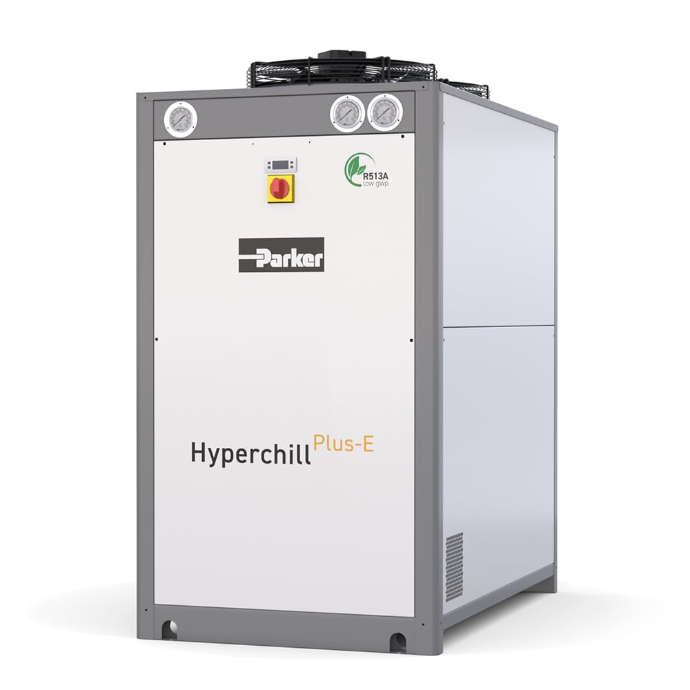
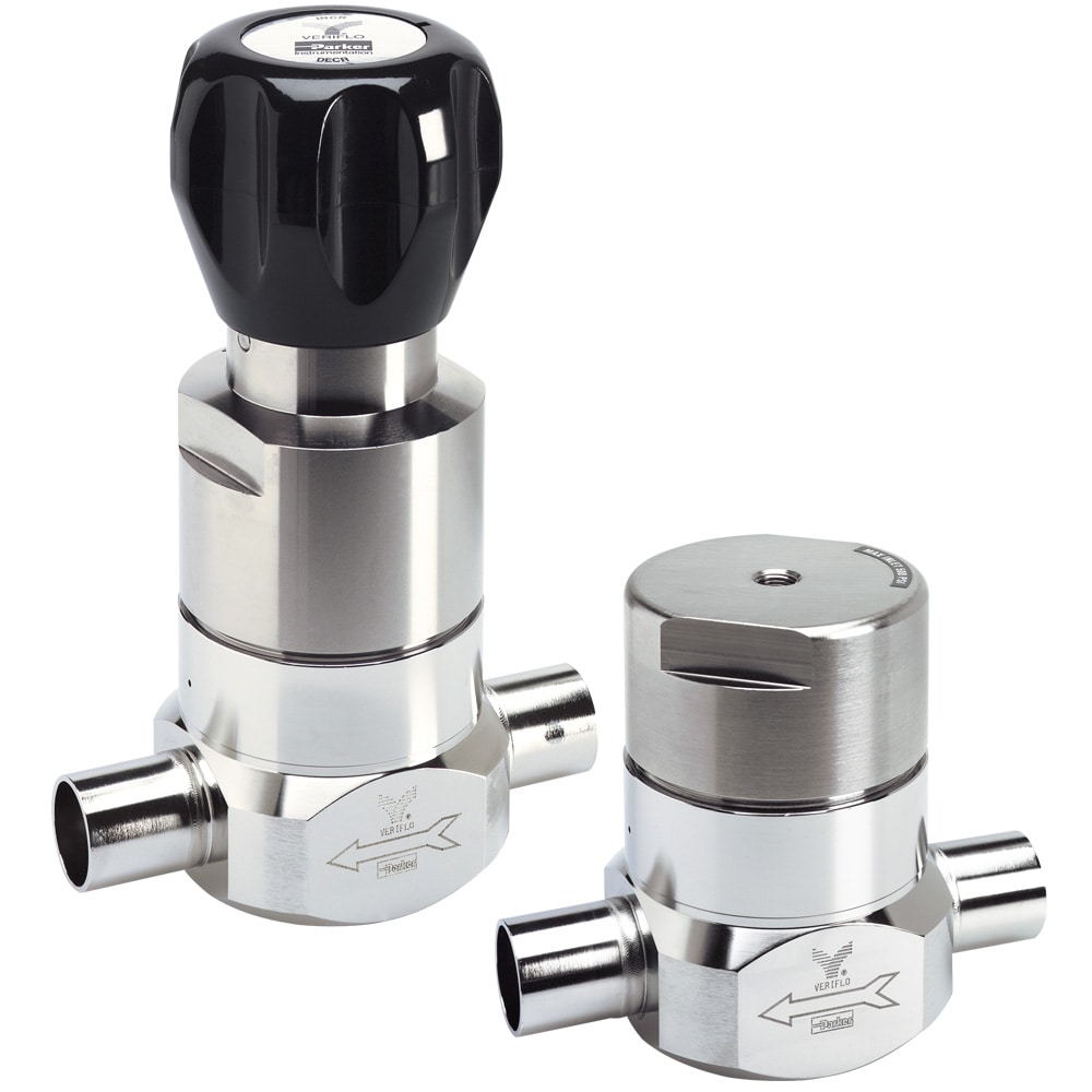
Machine tools for deposition and epitaxy need precise control and high purity, requiring high-purity fittings, valves, and pressure regulators. Fluid conveyance systems deliver precursor gases and liquids to the reaction chamber with precise flow control for uniform deposition or epitaxial growth. Sealing technology maintains vacuum or controlled atmospheric conditions and prevents leaks.
Electromechanical systems provide fine control for substrate positioning, temperature regulation, and precise flow control of gases and liquids, ensuring optimal conditions for the processes. Filtration technology ensures that all gases and liquids are contaminant-free, crucial for producing high-quality films and crystalline layers without defects.


Lithography
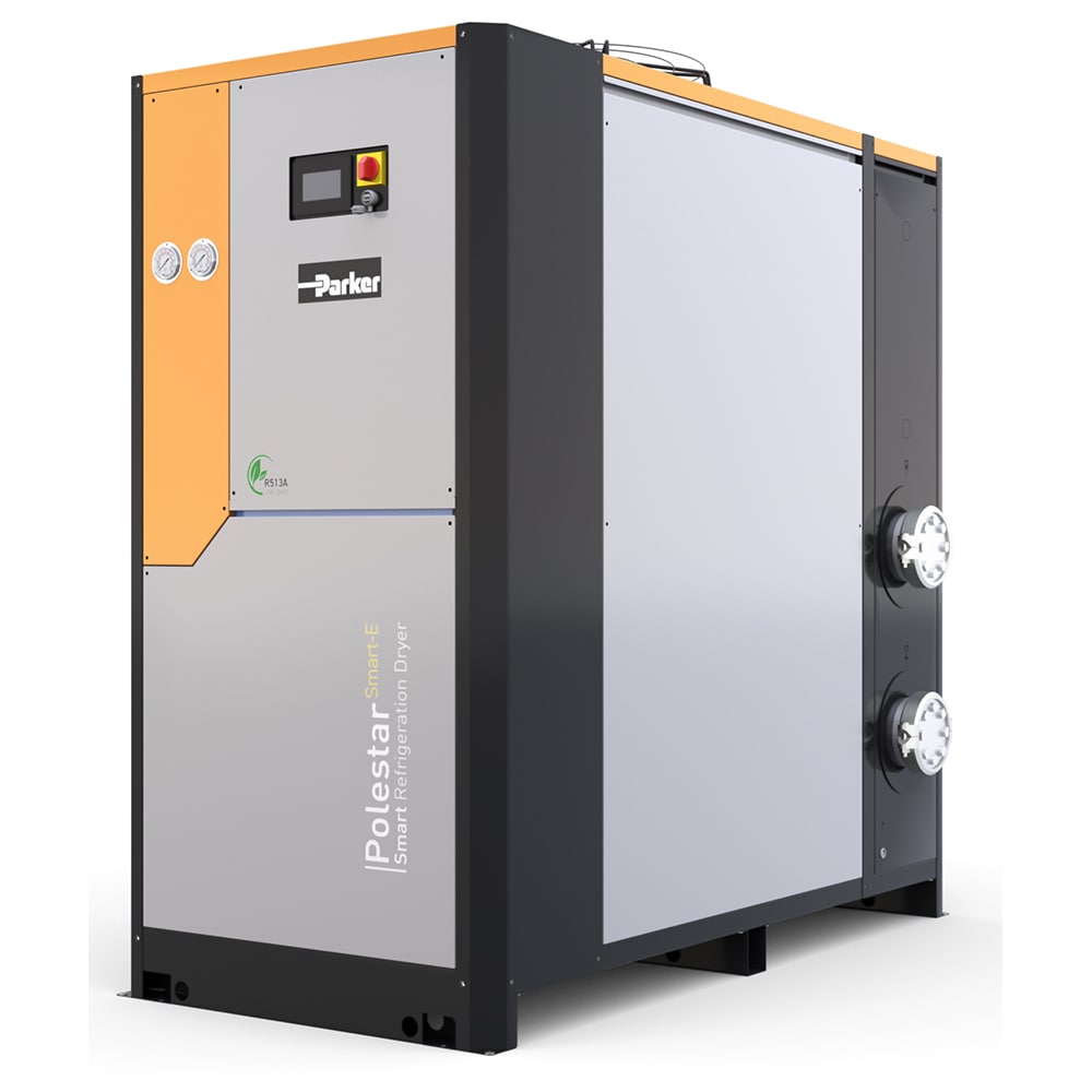
Lithography machines are essential in semiconductor manufacturing for patterning silicon wafers. These gigantic machines demand precise control and high purity, achieved through various integrated systems that are used in reticle handler, reticle stage, wafer handler, wafer stage, illuminator, source/facilities and protection options. Parker’s integrated core technologies ensure these machines operate with the necessary precision and purity, enabling the production of intricate semiconductor devices.
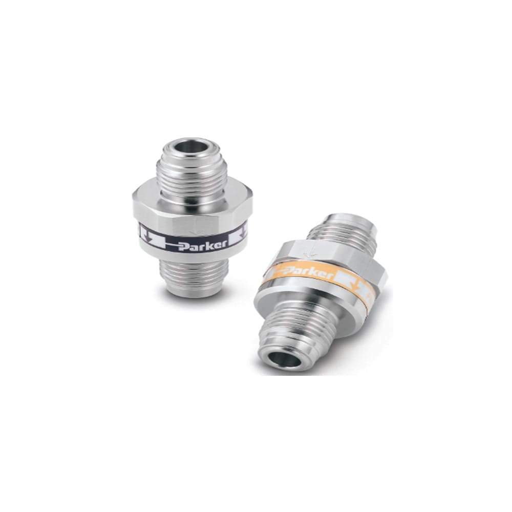
Fluid conveyance systems, including valves, hoses and UHP stainless steel fittings such as VacuSeal™, deliver cooling fluids to maintain temperature stability and transport photoresist with high precision. Sealing is crucial for maintaining the vacuum environment within the exposure chamber and preventing leaks in fluid and gas delivery systems. Parker’s metal seals ensure leak prevention and contamination control, preserving the required high purity and vacuum conditions.
Electromechanical systems offer fine control for wafer and photomask alignment and precise wafer stage movement during exposure. Filtration technologies ensure that all fluids and gases are contaminant-free, which is vital for high-resolution patterning and defect prevention.


Etching
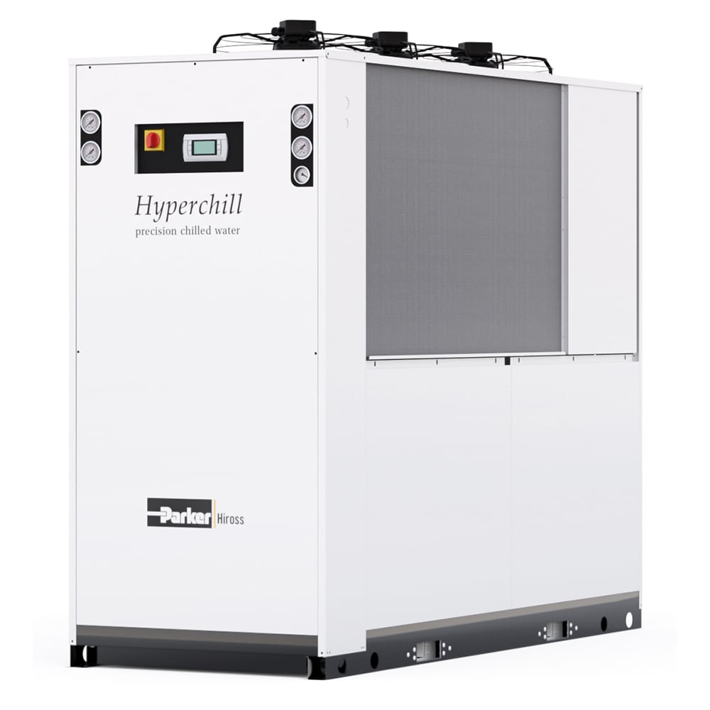
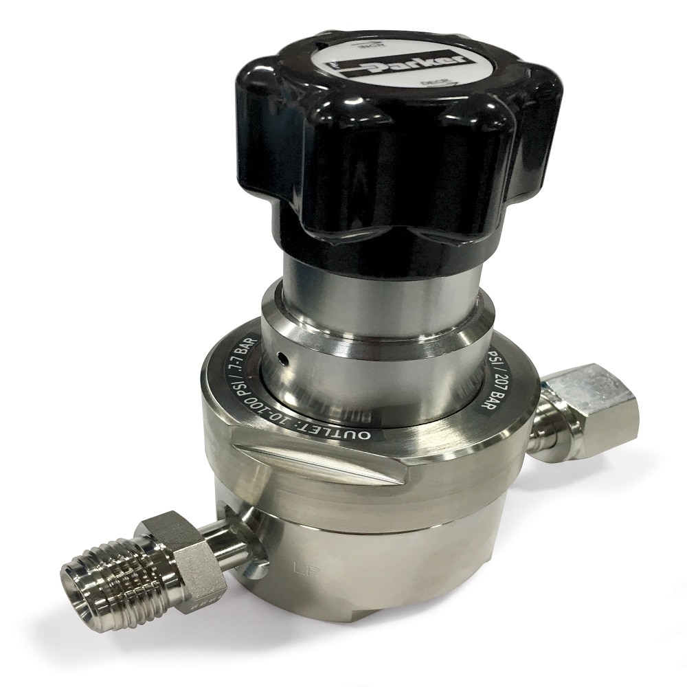
Etching selectively removes material from a wafer's surface to create patterns and structures. This process relies on fluid connectors, sealing, electromechanical components, and filtration technologies to ensure precision, purity, and reliability.
Fluid conveyance systems deliver etching gases and liquids with precise flow control, ensuring consistent etching. High-purity tubing, fittings, and connectors prevent contamination. Sealing technology maintains vacuum or controlled atmospheric conditions within the etching chamber and prevents leaks in gas and liquid delivery systems. High-quality seals handle the corrosive nature of many etching chemicals.
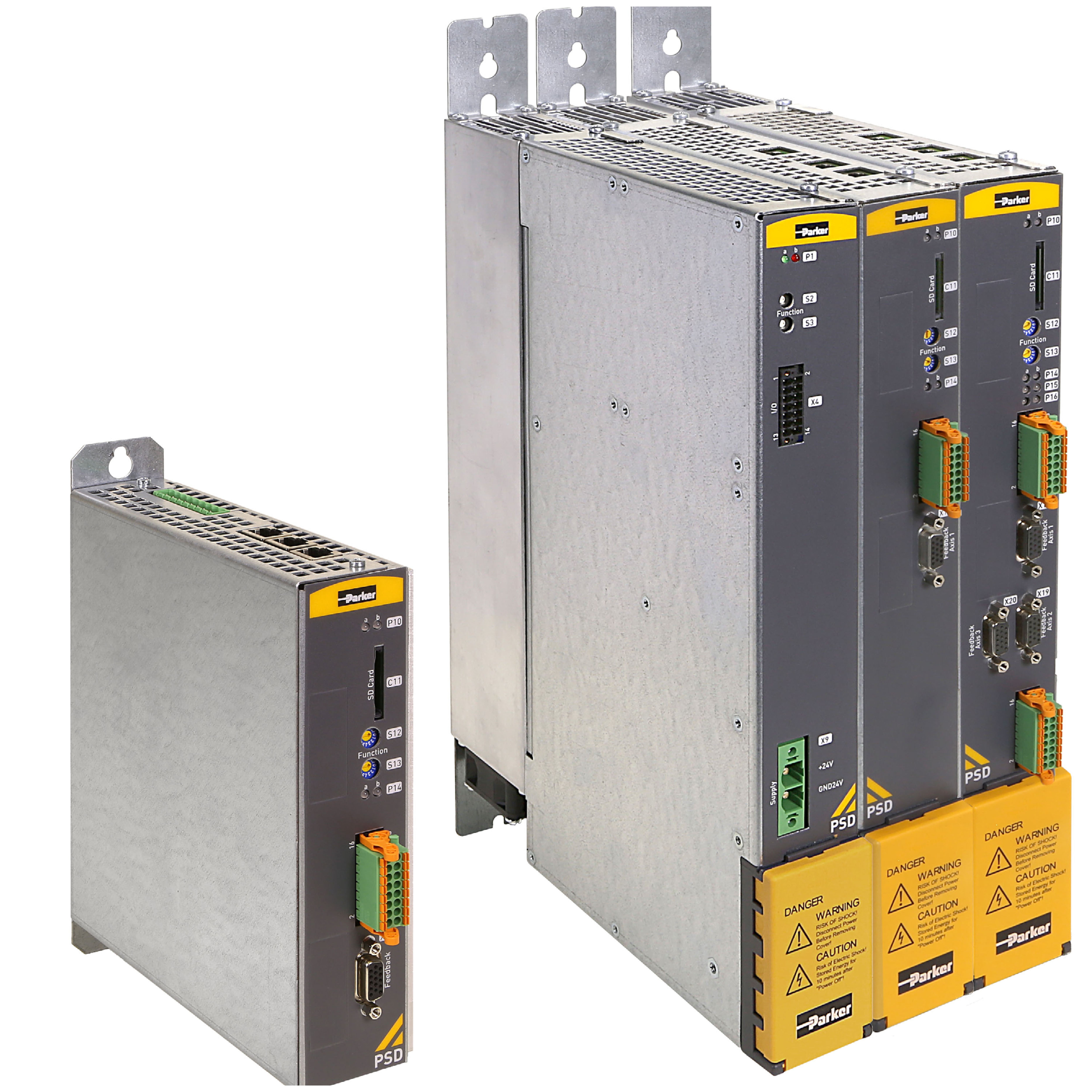
Electromechanical systems provide fine control for wafer positioning, flow regulation, and pressure maintenance, ensuring optimal etching conditions and achieving the desired patterns.
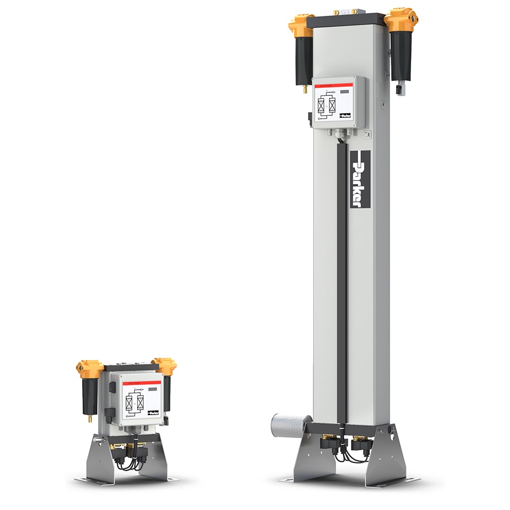
Filtration ensures that all gases and liquids used are free from contaminants, which is vital for precise and defect-free etching. This includes gas and liquid filters that remove impurities and particulates, as well as air filters that maintain cleanroom standards.
Ion Implantation
Ion implantation is the process of introducing dopants into silicon wafers to alter their electrical properties. It requires precise ion beam control and environmental conditions to achieve accurate doping levels and uniformity. Parker’s core technologies ensure reliability, precision, and purity in ion implantation.
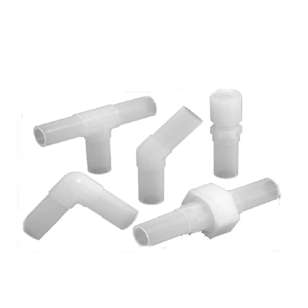
Fluid conveyance systems deliver precursor gases and cooling fluids to the ion source and other components with precise flow control, ensuring consistent ion implantation. High-purity tubing, fittings, and connectors prevent contamination. Sealing is crucial for maintaining vacuum or controlled atmospheric conditions within the ion implantation chamber and preventing leaks in gas and fluid delivery systems. High-quality seals handle high-vacuum environments and corrosive precursor gases.
Electromechanical systems provide fine control for wafer positioning, ion beam steering and focusing, and flow regulation, ensuring optimal conditions for achieving desired doping levels and uniformity.
Filtration technology ensures that all gases and cooling fluids used are contaminant-free, which is essential for precise and defect-free ion implantation. This includes gas and liquid filters that remove impurities and particulates, as well as air filters for maintaining cleanroom standards.

Cleaning
Cleaning is essential to remove contaminants using solvents, acids, or bases. RCA cleaning is a common method involving multiple steps to ensure wafer surface purity. Cleaning systems depend on robust filtration to maintain the purity of cleaning solutions and prevent contamination. Liquid Filters typically remove impurities from chemicals and water.
To support these processes, PTFE hose and tubing offer high chemical resistance, ensuring no degradation or leaching of contaminants into cleaning solutions. LIQUIfit® fittings provide leak-free connections that prevent contamination, maintaining the purity of the cleaning solutions. UHP PFA pressure vessels are designed to handle aggressive chemicals, ensuring that cleaning solutions remain pure and uncontaminated. Additionally, UHP CASY custom manifold assemblies manage the distribution of chemicals and gases with precision, preventing the introduction of contaminants.


Chemical Mechanical Planarization (CMP)
Chemical Mechanical Planarization (CMP) is a polishing process combining chemical and mechanical forces to smooth and planarize the wafer surface, which is crucial for multi-layered device fabrication. CMP tools typically use electromechanical components for precise control of polishing processes and filtration systems to manage slurry purity.


Wafer Handling Systems
Wafer handling systems are crucial in the semiconductor industry, ensuring precise and contamination-free transport, processing, and storage of silicon wafers. These systems use advanced technologies to maintain wafer integrity and quality.
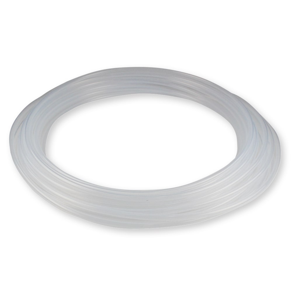
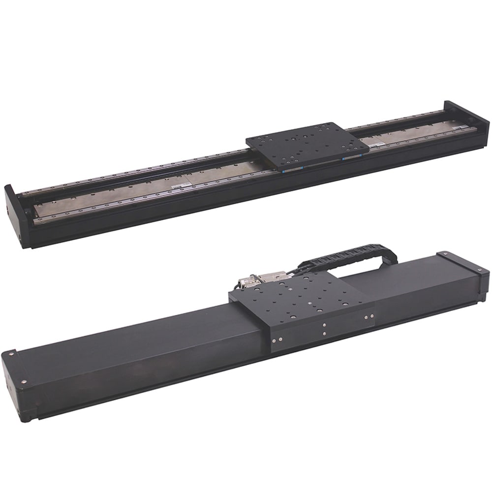
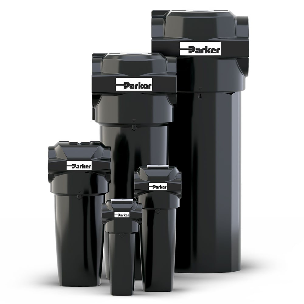
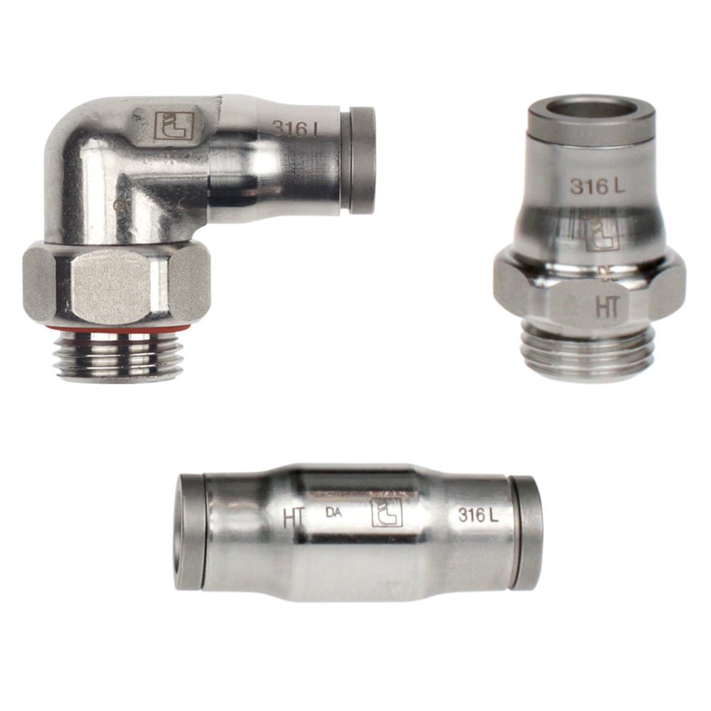
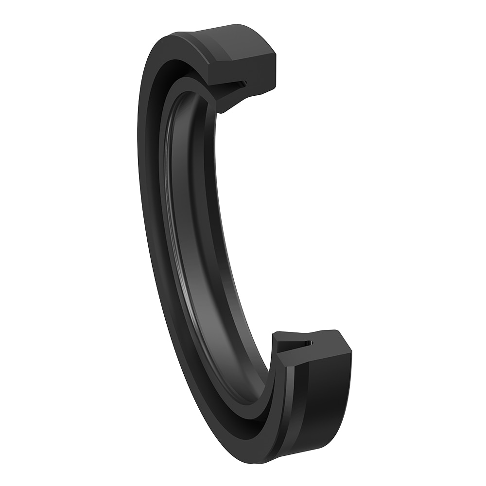
High-purity elastomer seals, such as O-rings, piston seals, and gaskets, prevent leaks and contamination. Seals for pneumatic cylinders ensure reliable operation of automated components. Filtration systems, including HEPA and ULPA filters, remove contaminants from fluids and gases. Electromechanical technologies like robotic arms, wafer transfer systems, robotic end effectors, and automated guided vehicles ensure precise wafer movement and alignment, minimizing human intervention and reducing contamination risks. Additionally, plastic tubing is utilized for its flexibility and chemical resistance in various fluid transport applications.


BACK-END PROCESS
The back-end process, also known as assembly, packaging and testing, involves the steps after the wafers have been fully processed and the individual chips are ready to be separated, packaged, and tested. Specialized machine tools are involved in this process.
Hybrid Bonding
The hybrid bonding process is an advanced technique to achieve high-density interconnections between stacked dies or wafers. It is particularly important for applications requiring high performance and miniaturization, such as in advanced processors, memory devices, and various types of sensors.
Parker's fluid conveyance and filtration technologies ensure the clean and precise delivery of bonding materials, while their process control systems enable the creation of more compact and efficient semiconductor devices by allowing for tighter integration and higher interconnect density compared to traditional bonding methods.
Chip First (InFO)
Integrated Fan-Out (InFO) technology involves placing the chips on a redistribution layer before encapsulation, allowing for better electrical performance and thinner packages.
Parker's electromechanical solutions provide the precise motion control needed for accurate placement of chips, and their filtration systems maintain the purity of materials used in the redistribution layer, thereby enhancing the overall reliability and performance of the final packages.
Chip Last (CoWoS)
Chip-on-Wafer-on-Substrate (CoWoS) technology involves mounting chips onto a wafer and then attaching the entire assembly to a substrate, enabling high-density interconnects and improved thermal performance.
Parker's advanced process control and fluid conveyance technologies are integral in maintaining the exact conditions required for this complex assembly, while their electromechanical systems ensure precise alignment and attachment of components, resulting in superior thermal and electrical performance of the semiconductor devices.